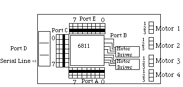
A 6811 microcontroller has 5 8bit ports used for input/output. the ports are identified alphabetically as Port A through Port E. On a Miniboard, these ports are dedicated to specific functions.
Port C is used for digital input or output. Each of the 8 bits on port C have a 3 pin plug associated with the bit on the Miniboard.
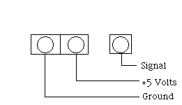
The plug provides +5 Volts, Ground, and Signal. The Signal pin is of most
interest because that is where the information will be present. Each bit in
Port C may be used either for an input or an output. The Data associated
with Port C is in the special register, PORTC, at memory location $1003. If
the bits of Port C are configured to be input, simply load the memory
location into an accumulator as in:
LDAA $1003
and what ever signals were present on the 8 pins of Port C will be read as
a one or zero value in the 8 bits of register A.
If the bits of Port C are configured to be outputs, simply write a byte to
memory location $1003 and the Signal pin of Port C will reflect the value
you just wrote.
	      LDAA	$%10101010
	      STAA	$1003
To configure the bits of Port C as either input or output, use the special
register DDRC (Data Direction Port C) at memory location $1007. Putting a
one in bit zero of DDRC will configure bit zero of Port C to be an output
whereas a zero in bit zero of DDRC will configure bit zero of Port C to be
an input. So each bit of Port C may be individually selected to be an input
or an output, and may be changed any time during program execution by
simply rewriting to DDRC ($1007).
Port D is used for serial communication and for Small Peripheral
Interface communications. Programs written and assembled on a PC must be
down loaded into the Miniboard's EEPROM. There is usually no other need to
implement serial communication. A downloading program on the PC will handle
all setup and serial communication during the download process. And SPI
communications would only possibly apply to multiple Miniboards which
needed to be networked together.
Port E is the analog input port. When a programmer wishes to
acquire data from an analog type sensor (like a photo-resistor, temperature
sensor, or an infrared detector), the A/D system of Port E is used. All 8
pins of Port E can sample analog (varying) voltages ranging between one and
+5 volts, and convert that signal to an 8 bit word which reflects the
strength of the voltage. An analog sample which results in a digital
reading of $00 signifies that a voltage level of 0 volts was present on
that channel during the sample. A digital reading of $FF signifies a
voltage of +5 volts. Any value between $00 and $FF is scaled to represent a
signal strength of somewhere in-between 0 and 5 volts.
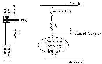
Developing external circuits, so that an analog sensor will produce a signal ranging between 0 and +5 volts requires some simple circuits knowledge. There are basically two types of circuits depending on whether the sensor is a resistive type device or a transistive type device. First, understand that the Miniboard has a part of the circuit in place already, a 47K ohm resistor pull-up device between the signal input pin and the +5 volt rail.
For a resistive circuit, the designer needs to implement a voltage divider circuit where the sensor is a variable resistor and the second resistor is the Miniboard's 47K ohm resistor. The simplicity of this circuit could not be greater. The designer need only plug in the sensor directly into an analog port socket.
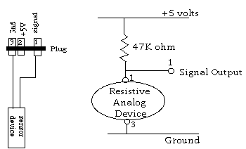
A resistive analog device varies in resistance. When its resistance is very small, the 47K resistor drops almost all of the 5 volts. This means that the signal output will be very near 0 volts. On the other hand, if the resistive analog device is producing a very large resistance (approaching an open circuit) then it will drop almost all of the 5 volts leaving the output signal at very near 5 volts.
If, during testing and calibration, the designer finds that the 47K ohm resistor is undesirable, and wishes a different valued resistor, then the circuit could be altered. The alteration is different for the cases of realizing a resistance less than 47K ohms and greater than 47K ohms.
To reduce the resistance below 47K ohms, place another resistor (R) in parallel with the Miniboard's 47K ohm resistor. The parallel combination of R and the Miniboard's can be made to vary between nearly 0 ohms, up to nearly 47K ohms.
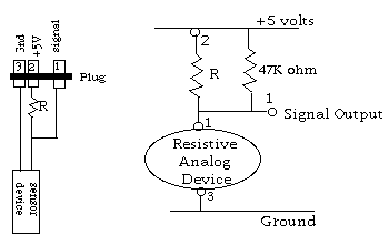
To increase the resistance above 47K ohms, place another resistor (R) in series with the Miniboard's 47K ohm resistor. The series combination of R and the Miniboard's resistor can be made to vary from, just above 47K ohms to as large as wanted.
For a transistive analog sensor device, the circuit designer's goal is to properly bias a transistor so that it will move into and out of saturation (i.e.... vary between on or off) based on desirable sensor input.
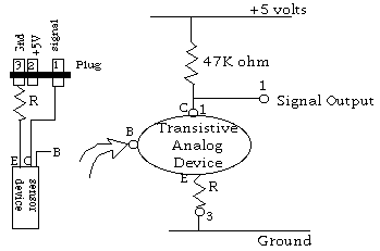
Here the transistive device is biased on the Collector by the Miniboard's 47K ohm resistor. A value other than 47K ohms (biasing on the collector) may be achieved as show in the previous examples with the resistive devices. A transistive device may or may not need to also be biased on the Emitter (probably not) by another resistor (R). The Base of a transistive device is left unconnected to the circuit because the environment provides the input to the Base. This is how the sensor operates. A properly biased transistor will vary between a very good conductor to a very poor conductor (we say "saturated" or "unsaturated") depending upon the Base voltage.
Since the environment controls the Base voltage, a circuit designer must bias the transistor so that what ever Base voltage swing is present in the environment will saturate and unsaturate the transistor. When the transistive device is working properly, it will be either a fairly high resistance, or a fairly low resistance. Then you can think of the circuit as a voltage divider.
Building sensor circuits is only half of the battle. The Miniboard programmer must still configure the A to D system to read values from the sensor.
Configuring Port E requires setting up several special registers. The
simple programming strategy to deal with the analog system would be to
acquire either the minilib by Fred Martin, or the libmb by Chuck Manis and
make calls to the library routine to acquire a digital value from an analog
port. Both of these libraries are available via ftp at
cherupakha.media.mit.edu/pub/miniboard/...
But the serious Miniboard programmer will want to know how to configure the A/D system and acquire values for him/her self. Configuring the A/D system requires powering up the A/D portion of the MCU (normally it is off and not drawing current) and specifying which channel to convert and how many times to convert it. Here is an example of code:
analog: EQU *
ldaa port *get port # into a
staa ADCTL,x *Start an A to D conversion
convert:
ldaa ADCTL,x *wait
anda #$80 *wait
beq convert *wait until conversion is complete
* *(takes 128 cycles)
ldab ADR1,x *return result in Acc B
stab PORTC,x *send to output on PortC
bra analog *endless loop
******************* Vectors (Reset Only)***********************
ORG $FFFE
RESET FDB setup Point to start of program
end
BASE EQU $1000
PORTC EQU $03 * Port C data register
DDRC EQU $07 * Data Direction register for port C
ADCTL EQU $30 * A/D Control/status Register
ADR1 EQU $31 * A/D Result Register 1
OPTION EQU $39 * system configuration Options
CONFIG EQU $3F * Configuration Control Register
******************* variables (RAM) section **********************
ORG $00
port rmb 1
******************* Code (EEPROM) Section ************************
ORG $F800
setup: equ *
sei *no interupts during this program
ldx #BASE
bset OPTION,X $80
ldaa #$ff
staa CONFIG,x *turn on analog subsystem
staa DDRC,x * = output (suggest LEDs)
ldaa #$02 ********start looking at analog port # 2 ***
staa port
First the A/D system is powered on by writing a 1 to bit 7 of the OPTION
Special Register at memory location $1039. All the rest of configuration
takes place in the ADCTL Special Register at memory location $1030. Bit 4
of ADCTL is the 'MULT' bit which will select between converting a single
channel 4 times in a row (if set to 0), or converting 4 channels once (if
set to 1)... either way, four results are returned by the A/D system. The
results are returned in the Special Registers ADR[1->4] at memory locations
$1031 -> $1034. Bit 5 of ADCTL is the 'SCAN' bit which will select between
doing four conversions and then stopping (if set to 0) or continuously
converting without ever stopping (if set to 1). Bit 7 of ADCTL is a 'CCF'
(conversion complete flag). This bit is set by the A/D system when an A to
D conversion is completed. Bits 0, 1, and 2 of ADCTL will select which
channel or channels to convert and return results for. In the case that the
programmer wishes to convert a single channel 4 times (Set MULT to 0) then
writing a %000 to ADCTL bits 0, 1, & 2 will convert channel 0 (i.e.... the
analog sensor which is nearest to the power supply). Writing a %111 to
ADCTL bits 0, 1, & 2 will convert channel 7 (i.e.... the analog sensor
which is nearest to the serial port). Any channel (port E sensor) may be
selected by writing it's channel number (0 through 7) to ADCTL bits 0, 1,
&2.
ieeecs@hal.elee.calpoly.edu